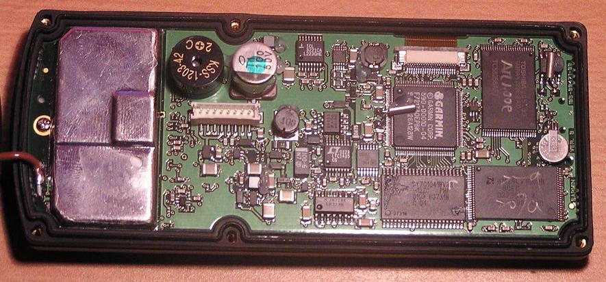
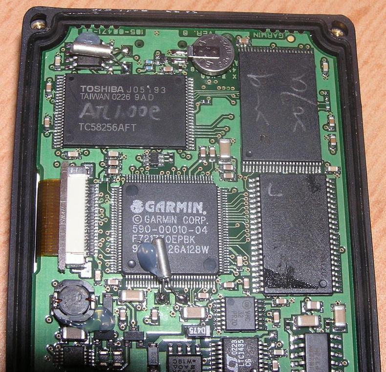
These are the memory chips used:
AM29LV160BB-90 - 16 Mbits Flash (1Mx16) 3.3V
CY7C1041BV33-12 - 4 Mbits SRAM (256Kx16) 3.3V
TC58256 - NAND Flash (32Mx8) 3.3V (TSOP48)
The first flash holds the firmware for their 16 bit processor (ARM core) and the third one holds
the base map and the downloaded maps.
There are many other Flash NAND memory chips with 64M/128M/256M capacities which are pin to pin compatible and command compatible. The only difference between them is the address cycle. For the 32M versions the data bus pulses 3 times to send A0-A7, A9-A16, A17-A24 For the bigger capacity versions a 4th cycle is needed to send A25-Ax. The lower capacity NANDs ignore the 4th cycle address so all these memories could use the same (4 cycle) address sending subroutine.
Updated 09 Aug 03
Well, I haven't hooked the logic analyser but I did a much better thing, I've disassembled the firmware. To be more precise the processor has an ARM7 core (r13=sp, r15=pc) and the code was nasty to disassemble because it supports two simultaneous encodings: "Thumb" which is a 16bit encoding and the normal 32bit encoding. This made the disassembly process quite painful because I had to tell my Interactive Disassemble when it couldn't guess by itself when to switch from one to the other. Since this was a ROM image the data was mixed with the code and also needed my hints to disassemble correctly. Anyways after 3 hours of work I had a very raw listing. The processor runs a multi-threaded real time system with semaphores and more than 130K from the 1.5M of firmware are text messages translated from english to french, german etc.
The very good news is that I've found the following structure in firmware:
DCB 0xA4, 0, 0, 0, 0, 0x6F, 1, 4, 0, 0, 0, 0, 0, 0, 0, 0, 0, 0, 0, 0
DCB 0xEA, 0, 0, 0, 8, 0x6F, 1, 4, 0, 0, 0, 0, 0, 0, 0, 0, 0, 0, 0, 0
DCB 0xE5, 0, 0, 0, 0x10, 0x6F, 1, 4, 0, 0, 0, 0, 0, 0, 0, 0, 0, 0, 0, 0
DCB 0xE3, 0, 0, 0, 0x10, 0x6F, 1, 4, 0, 0, 0, 0, 0, 0, 0, 0, 0, 0, 0, 0
DCB 0xE6, 0, 0, 0, 0x18, 0x6F, 1, 4, 0, 0, 0, 0, 0, 0, 0, 0, 0, 0, 0, 0
DCB 0x73, 0, 0, 0, 0x20, 0x6F, 1, 4, 0, 0, 0, 0, 0, 0, 0, 0, 0, 0, 0, 0
DCB 0x75, 0, 0, 0, 0x28, 0x6F, 1, 4, 0, 0, 0, 0, 0, 0, 0, 0, 0, 0, 0, 0
DCB 0x76, 0, 0, 0, 0x30, 0x6F, 1, 4, 0, 0, 0, 0, 0, 0, 0, 0, 0, 0, 0, 0
DCB 0x79, 0, 0, 0, 0x38, 0x6F, 1, 4, 0, 0, 0, 0, 0, 0, 0, 0, 0, 0, 0, 0
If you compare this with a fragment of code from the Linux MTD driver:
struct nand_flash_dev {
char * name;
int id;
int chipshift;
unsigned long erasesize;
char page256;
};
struct nand_flash_dev nand_flash_ids[] = {
{"NAND 1MiB 5V", 0x6e, 20, 0x1000, 1},
{"NAND 2MiB 5V", 0x64, 21, 0x1000, 1},
{"NAND 4MiB 5V", 0x6b, 22, 0x2000, 0},
{"NAND 1MiB 3,3V", 0xe8, 20, 0x1000, 1},
{"NAND 1MiB 3,3V", 0xec, 20, 0x1000, 1},
{"NAND 2MiB 3,3V", 0xea, 21, 0x1000, 1},
{"NAND 4MiB 3,3V", 0xd5, 22, 0x2000, 0},
{"NAND 4MiB 3,3V", 0xe3, 22, 0x2000, 0},
{"NAND 4MiB 3,3V", 0xe5, 22, 0x2000, 0},
{"NAND 8MiB 3,3V", 0xd6, 23, 0x2000, 0},
{"NAND 8MiB 3,3V", 0xe6, 23, 0x2000, 0},
{"NAND 16MiB 3,3V", 0x73, 24, 0x4000, 0},
{"NAND 32MiB 3,3V", 0x75, 25, 0x4000, 0},
{"NAND 64MiB 3,3V", 0x76, 26, 0x4000, 0},
{"NAND 128MiB 3,3V", 0x79, 27, 0x4000, 0},
... one can clearly see that it's the NAND flash structure with the corresponding device IDs.
This is a very clear indication that NAND flashes which are supported by
GPS V are all the 3.3V chips with sizes from 2MB to 128MB.
The manufacturers are any of the following four:
TOSHIBA (0x98), SAMSUNG (0xec), FUJITSU (0x04), NATIONAL (0x8f)
Now I'm very confident to change my NAND chip once I've copied the info from the old one. I do have some 64MB chips laying around but I would like to use a 128MB one which I have to order. I would rather not desolder/solder twice the memory. Depending on my mood tomorrow I will try with the 64M one or wait a couple of days to get the 128M chip.
Updated 20 Aug 03
I've finally managed to solder my new chip inside the unit too. I took the NAND chip from a Sony memory stick since it was half the price of a new NAND chip. Use a cutter and carefully open the memory stick package: http://nic.ath.cx/GPSV/mstick128.jpg and you've got yourself a cheap 128MB flash NAND chip.
I've also purchased a Dazzle 8in1 USB programmer (which works in Linux with the USB storage module) to transfer my basemap from the old chip to the new one. I've soldered wires from the Smartmedia connector to a DIP to TSOP48 adaptor but after testing with a dummy chip I've noticed data misalignment between read and writes. These are probably the result of my wires which are increasing the signals load and because the Dazzle programmer is a high speed one (USB 2.0). So I've postponed the basemap transfer for sometime later. I'm amazed that expensive programmers don't handle these flash NANDs since they are so easy to interface. One can always solder these chips into cheap USB programmers or pen drives to read/program them.
In your GPSV you'll find either a Toshiba TC58256AFT or a
Samsung K9F5608U0A-YCB0 chip (both are 32MB 3.3V NANDs).
You will want to replace this chip with any of the following:
Size Samsung Toshiba
64MB (512Mb) K9D1208U0A-YCB0 TC58512FT
128MB (1Gb) K9D1G08U0M-YCB0 TH58100FT
I've replaced mine with a 128MB chip directly taken out of a memory stick without even erasing it (so it had a few Sony strings and format data) and it is working fine.
The NAND flash holds _only_ the basemap and the other maps. All the other information like waypoints, track data and other settings are stored in the firmware flash since I haven't lost them after soldering the new chip.
As a conclusion: upgrading your memory chip is easy and harmless.
Now the Mapsource software side still needs some work.
While trying to load a larger set while it says "building index"
you will get the following error:
The map set is too large.
Please choose a smaller map set.
which is a unicode string from the file MapSource_Lang.dll
My guess is that the software doesn't even bother to query the unit's memory size and uses some fixed values. If you disconnect the serial cable from the unit right after its presence is detected the "building index" still goes on and finishes with the same error.
I've started the program's disassembly but just the initial
analysis takes a few hours and I'll need some more time
to figure this one out.
If I don't "fix" the Mapsource this week I'm afraid you'll
have to wait 3 weeks until I'm returning from my vacation.
- thanks to Matrix